SSPA 800W/1000W 144 MHz

Le transistor utilisé pour ce projet est un Freescale MRF6VP11KH
C'est un projet commun F6BKI / F1TE pour l'activité WSJT EME, pour ceux qui peuvent utiliser cette puissance....
L'ampli lui-même découle des notes d'application Freescale de ce produit.
Le prototype de la photo ci-dessous délivre 900W pour 3.8W d'entrée avec un rendement de 72%. Ceci est encourageant.
The transistor used for this project is a Freescale MRF6VP11KH
This is a common project F6BKI / F1TE for EME (CW-WSJT) and also Tropo applications.
The amplifier itself is based on an MRF6VP11KH Freescale application-note.
The prototype described below delivers 900W out for 3.8 W input with an
efficiency of 75%. This is a VERY ENCOURAGING first step.
Recently the MRFE6VP61K25H designed for Enhanced Ruggedness has been introduced.
It is capable of Handling a Load Mismatch of 65:1 VSWR, @ 50 Vdc,230 MHz, at all Phase Angles, 1250 Watts Pulsed Peak Power, 20% Duty Cycle, 100 μsec, and capable of 1250 Watts CW .
http://cache.freescale.com/files/rf_if/doc/data_sheet/MRFE6VP61K25H.pdf
http://www.marsport.org.uk/dubus/last.htm.
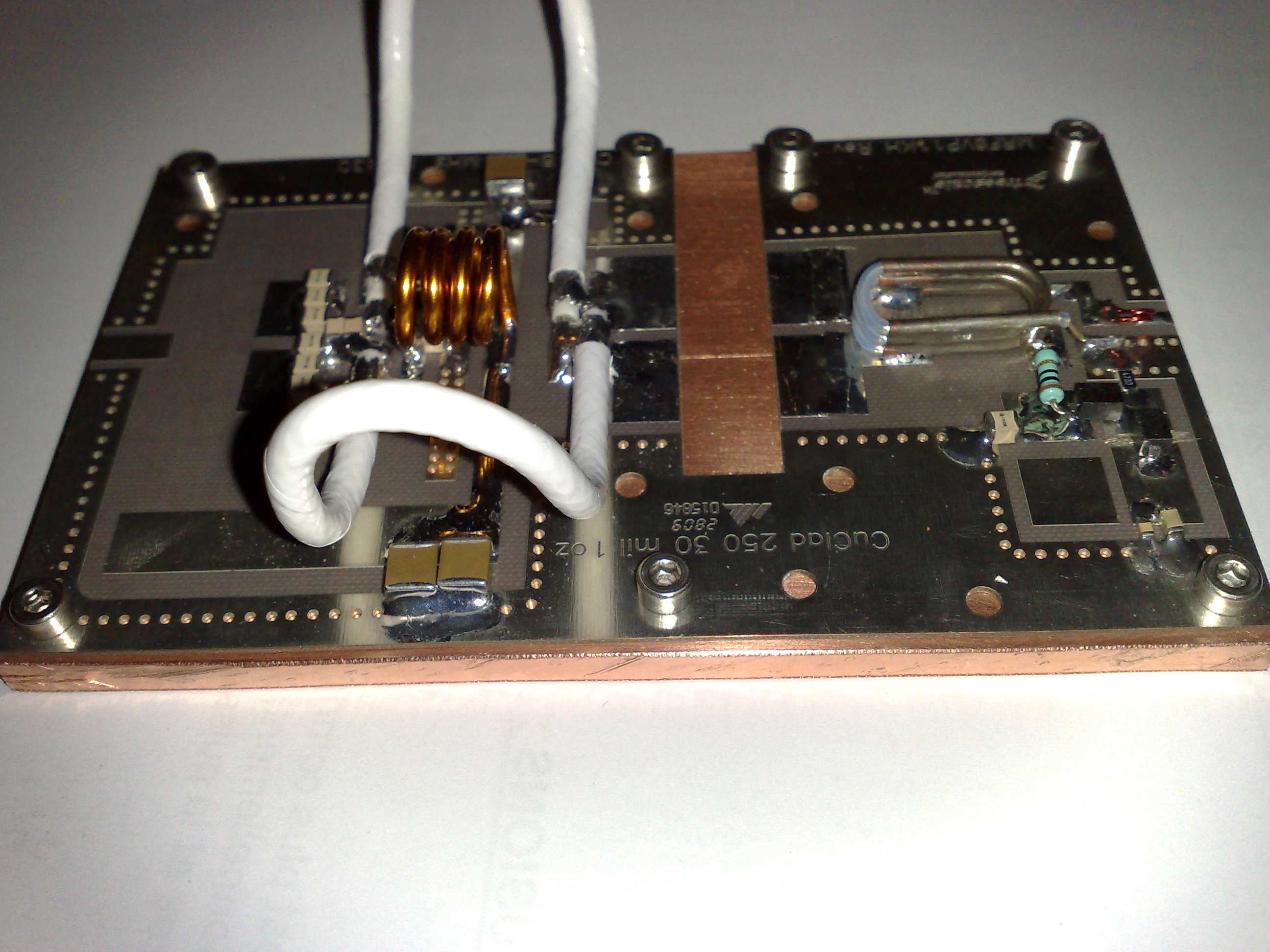
Prototype MRF6VP11KH
VD = 48V, IDQ = 250 mA
| RF power IN (W) | RF power OUT (W) | ID (A) | Power IN (W) | Efficiency % |
| 1.2 | 400 | 15 | 720 | 55.5 |
| 1.4 | 500 | 17.8 | 850 | 59 |
| 2 | 600 | 19.3 | 925 | 65 |
| 3 | 800 | 23 | 1100 | 72.5 |
| 3.8 | 900 | 25 | 1200 | 75 |
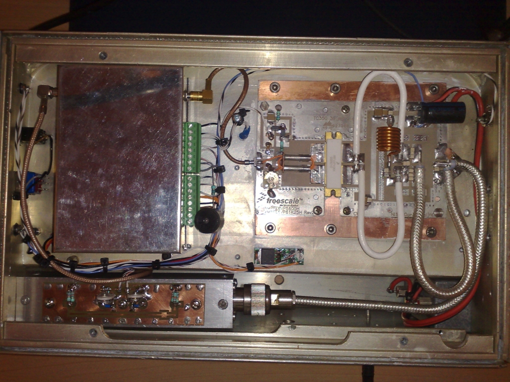
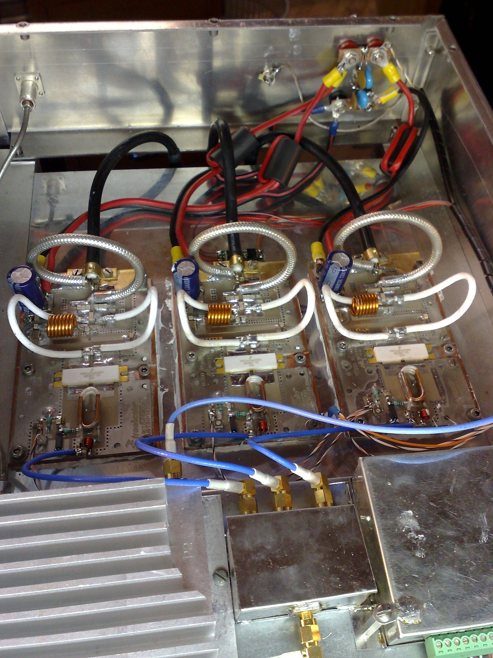
Another one SSPA with MRF6VP41KH
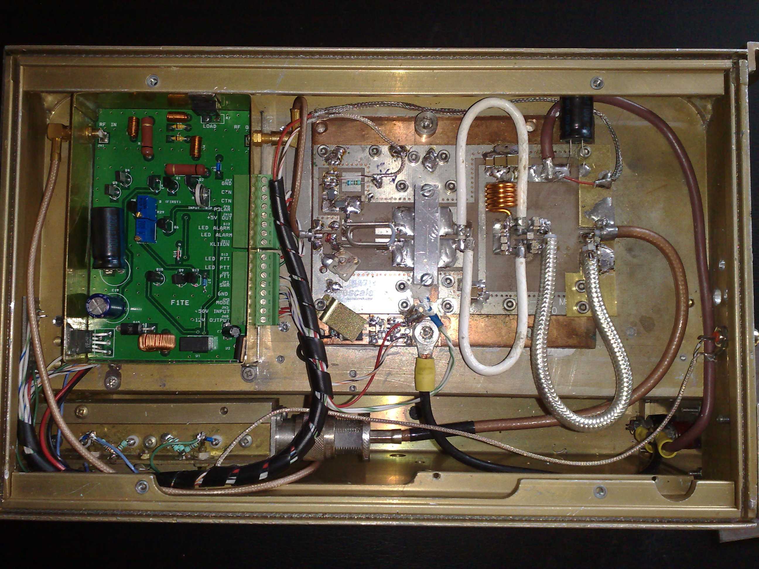
Autour ce cet ampli, un certain nombre de protections provoquent la mise en sécurité de l'amplificateur par commutation électronique donc avec un temps de réaction très rapide.
Les transistors Freescale de cette série acceptent une tension de blocage négative de quelques volts.
Une alarme déclenche le blocage du transistor en passant sa tension de polarisation à -3V environ.
L'alarme est mémorisée et sa RAZ ne peut se faire que par mise hors-tension.
Although this transistor is extremely robust by itself, some electronic protections have been implemented.
To reach this goal we have decided to make this electronic as simple as possible.
When an alarm is detected a negative voltage is applied to the gate of the transistor to reduce its gain and consequently its output power to a level where the transistor can handle high stress with no problems.
This negative voltage is –3 Volts, we know for sure that this negative voltage is OK with this specific Freescale transistor, it has been designed to operate in such conditions, and it might not be the case for other transistors.
The issue is that the Gate/Source voltage breakdown can be reach if the RF input drive is still applied on top of the negative gate voltage.
For the MRFE6VP61K25H there is no problem.
The alarms are stored and can be reset only by switching down the power supply.
Trois nivaux de protection :
The alarms are generated if the following parameters are exceeding a given value:
Un module de contrôle le niveau de la puissance d'entrée.
Input RF drive
e circuit à pour but de faire disjoncter l'amplificateur si la puissance d'entrée dépasse un certain seuil.
Ce seuil est ajustable par un potentiomètre.
The input RF level at which the alarm is activated is adjustable by a potentiometer.
Un module de protection thermique
Internal temperature
Raccordé à la carte de polarisation sur l'entrée "Klixon" il permet de déclencher la sécurité si la température du capteur dépasse un seuil déterminé.
Le transistor est bloqué, la puissance d'entrée est commutée sur charge.
A thermal protection module
A "Klixon" sensor, outside the protection board is used to activate the temperature protection.
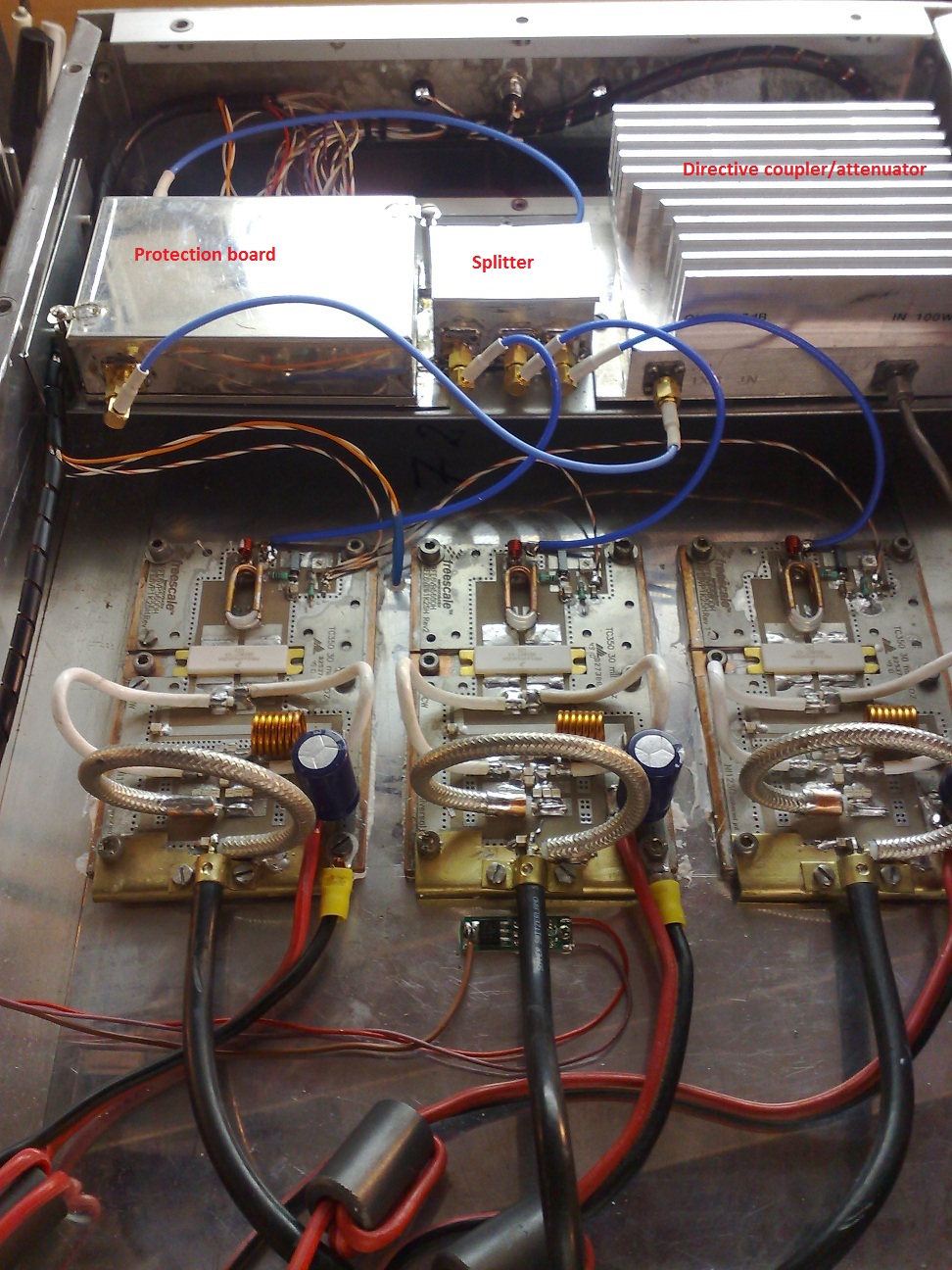
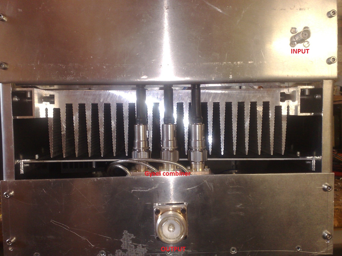
Un module de protection ROS de sortie.
Output load mismatches
Une sonde en sortie de l'amplificateur détecte les tensions directe et réfléchie.
Ces tensions sont comparées dans un circuit spécialisé dont la sortie en "bargraph' permet de sélectionner le seuil de ROS admissible pour déclencher l'alarme.
Si une protection déclenche la mise en sécurité du transistor, la RF d'entrée est commutée par diode PIN sur charge fictive.
L'ampli a été testé sans charge en ROS infini à 800W de sortie.
A high power coupler is used at the output of the amplifier to sense the direct and reflected RF power.
The corresponding DC voltages are compared by a dedicated circuit driving a "bar graph" indicator. Threshold levels for different output VSWR values can be selected to provide an alarm.
When any of the alarms is activated the input RF drive is switched to an internal load via a PIN Diode circuit, it also protects the TRANSCEIVER driving the amplifier.
This prototype has survived infinite output VSWR at an output level of 800W CW.
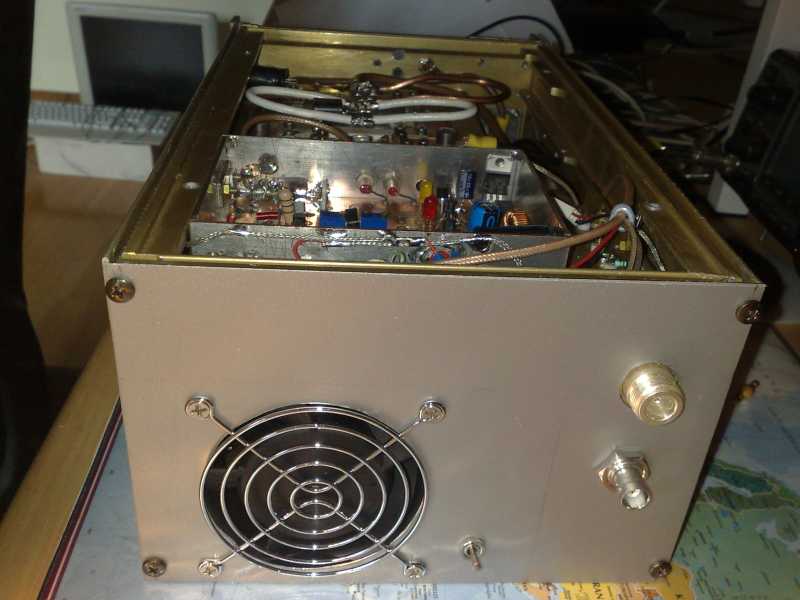
Réalisation
Le circuit imprimé ainsi que le transistor sont montés sur une semelle de cuivre de 5 mm d'épaisseur minimum.
De préférence souder à l'aide d'une plaque chauffante la totalité de la surface du circuit imprimé avant montage des composants,
Souder de la même manière le transistor. La dissipation thermique sera bien meilleure.
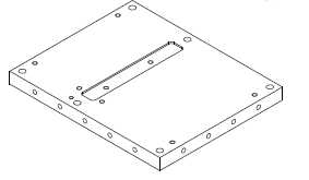
Disspipateur cuivre
Ari, OH7KBF, m'a fait parvenir un plan 3D d'un dissipateur cuivre pour ce circuit imprimé.
Il a été dessiné par Vesa OH4EA.
Un grand merci à tous les deux.
Je vous le met à disposition en format PDF.
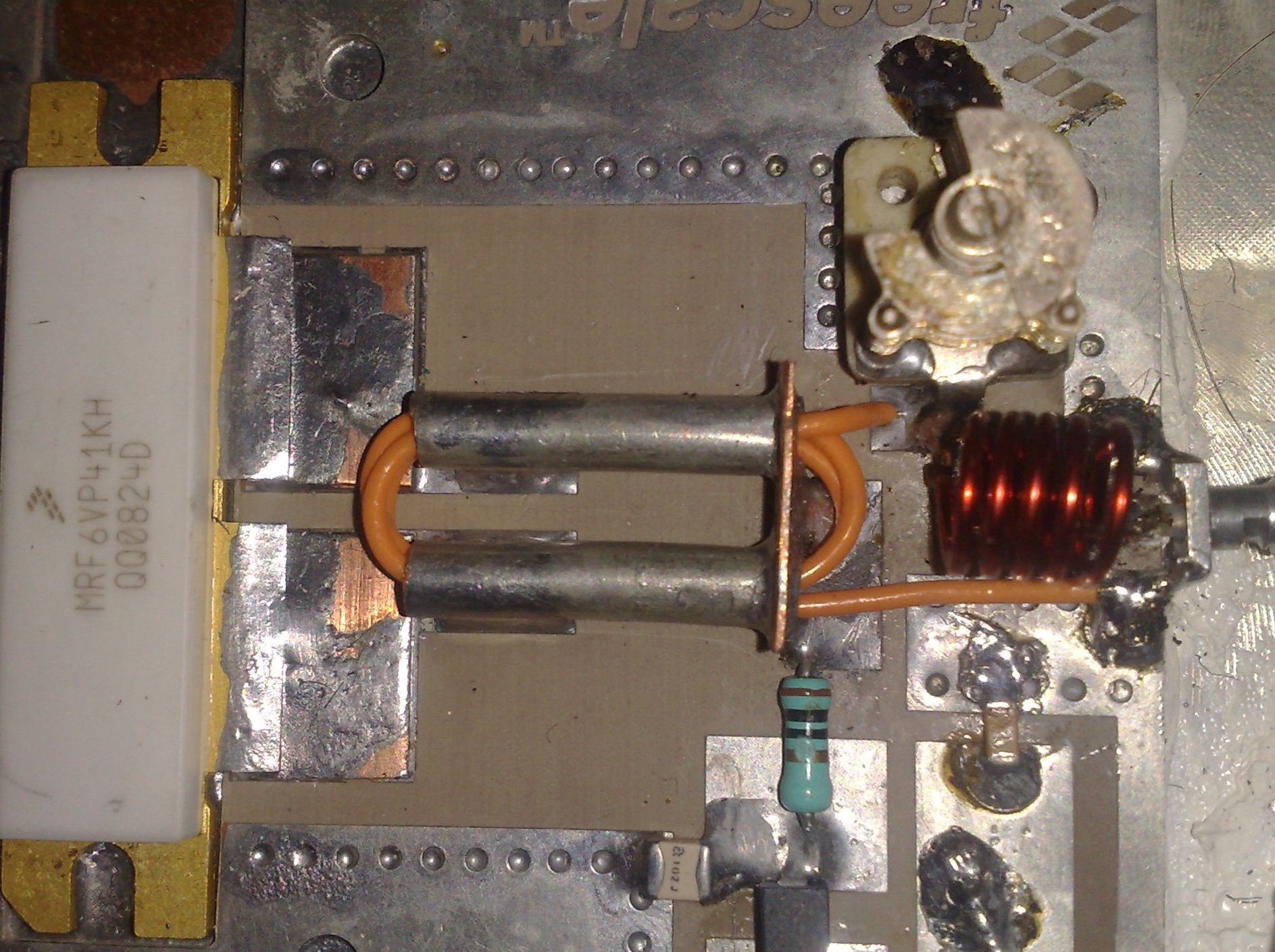
Transformateur d'entrée alternatif
Sur une idée de DL4XX, j'ai testé ce transformateur d'entrée qui donne les mêmes résultats et qui est plus facile à réaliser, et moins cher.
J'ai utiliser le conducteur extérieur cuivre d'un morceau de coaxail rigide en téflon de 3.6 mm.
Deux morceaux de 18 mm de long soudés ur un bout de feuille de cuivre et dans lequel j'ai bobiné trois spires de fil téflon.
L'adaptation se fait par une self de 5 tours, 8/10, diamètre 5mm et par un ajustable 15/20 pF.
Alternative input transformer
On an idea of Andreas, DL4XX, I tested the input transformer which gives the same results and is easier to make, and cheaper
I use the copper of the outer conductor of a 3.6mm rigid teflon coaxial.
Two pieces of 18 mm length welded on a piece of copper foil and in which I wound three turns of Teflon wire.
Adaptation by inductor in 8/10 enameled diameter 5mm and variable capacitor 5/20 pF.
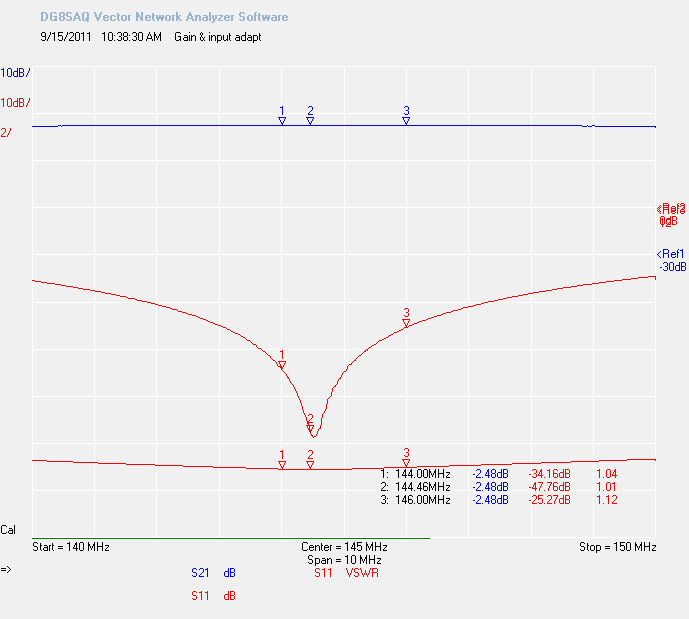
Input adaptation and gain in AB class
With 30dB power attenuator insert on output
G = 30-2.48 = 27.52dB
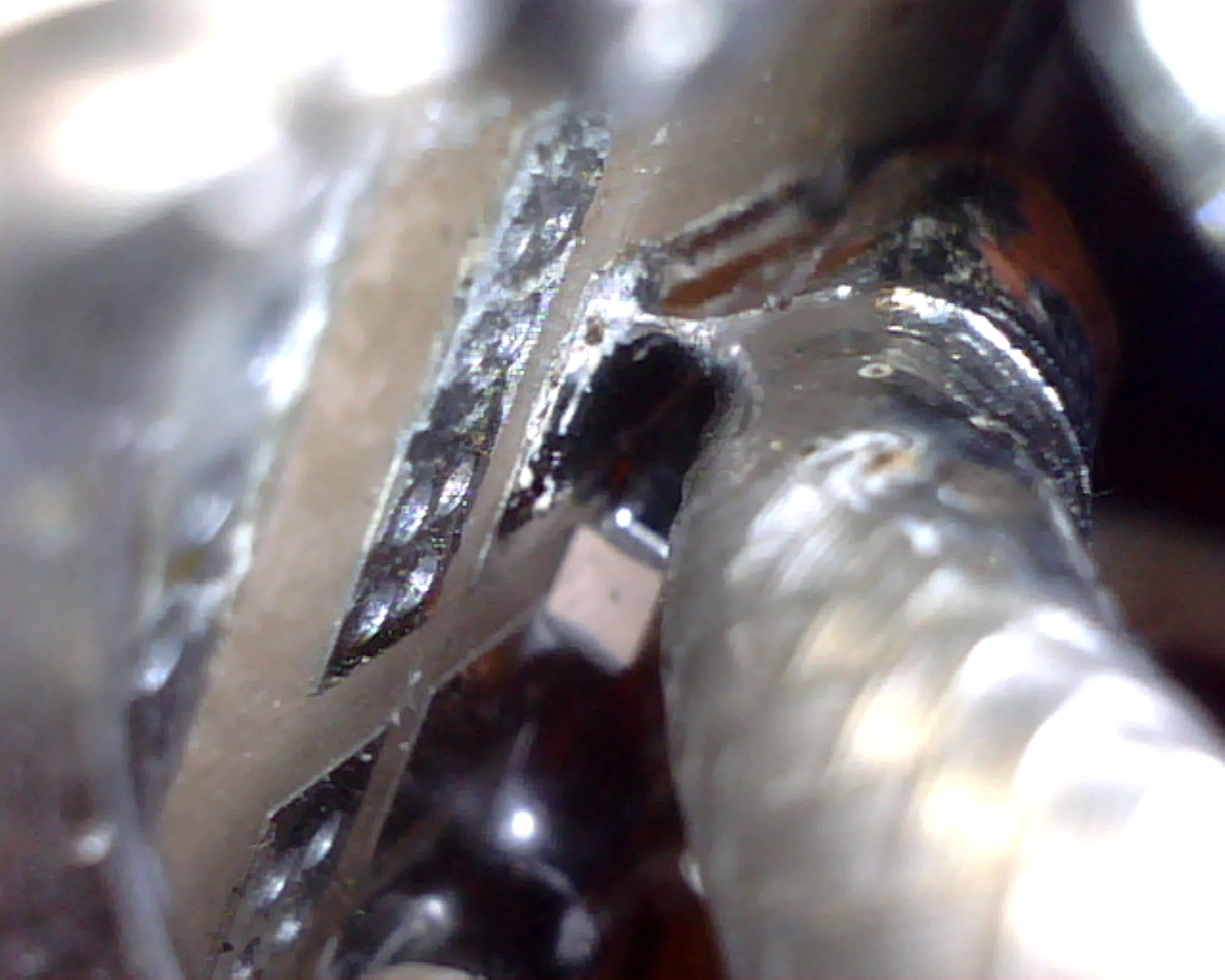
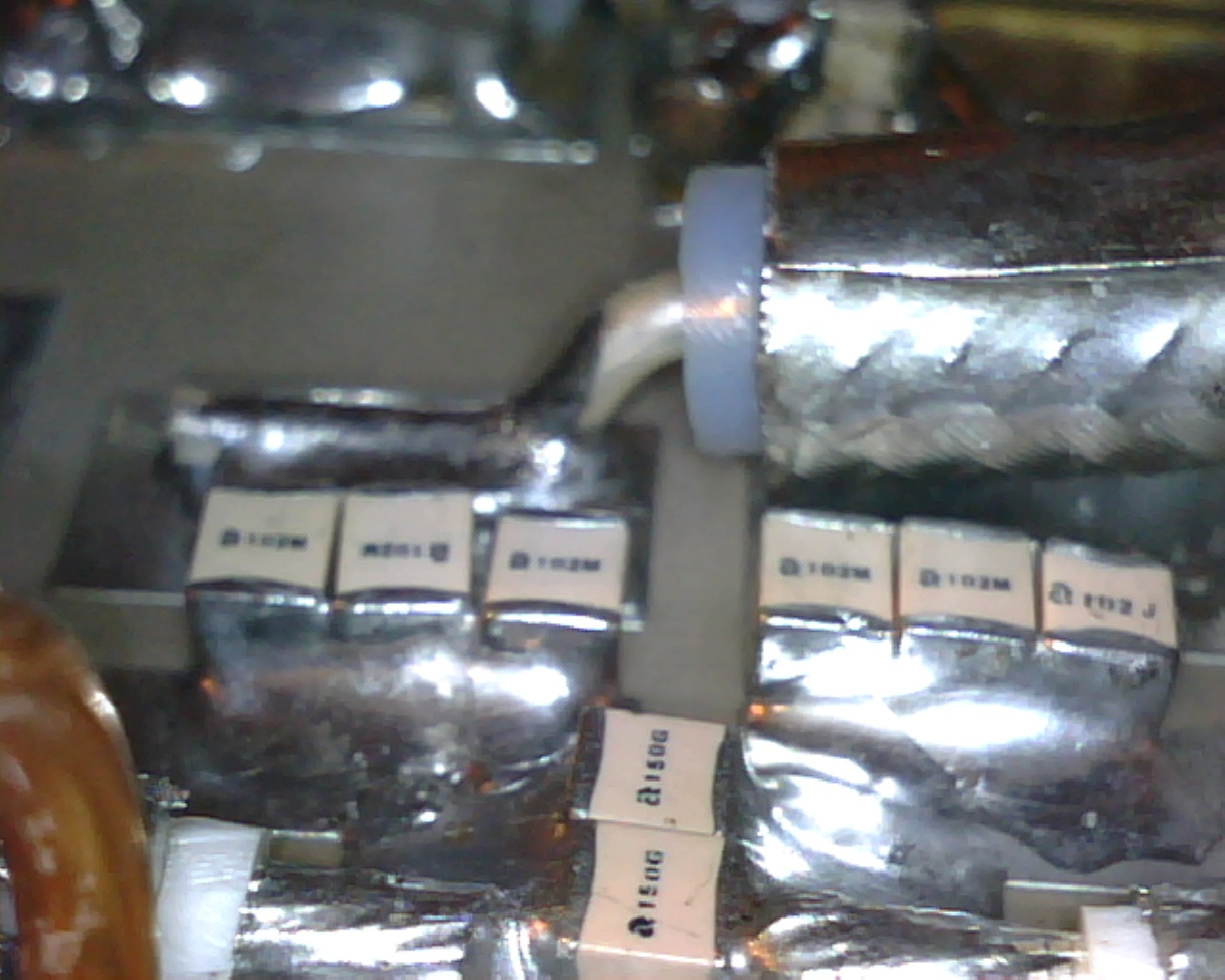
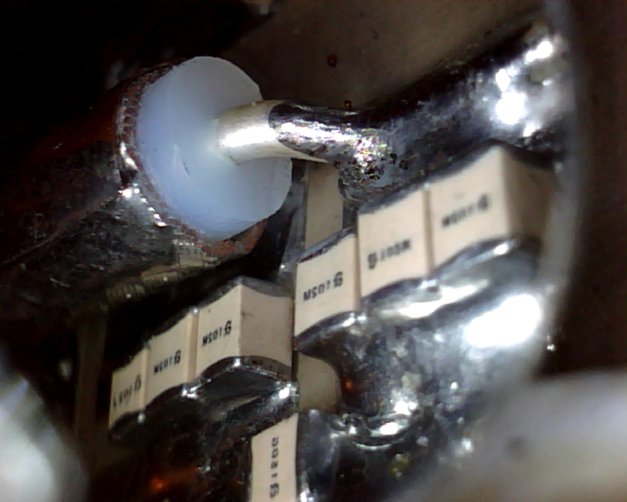
Protect output ATC capacitor from thermal constraints
do not soldering directly to the outer jacket of the output balun on ATC capacitor.
use a small sheet of copper for that